


Logic Box - Family Picture
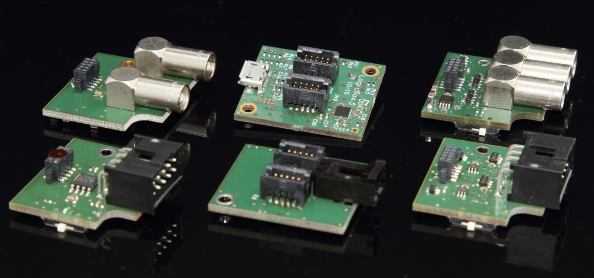
Here's a family picture of all the boards in the
Logicbox family. In the middle you can see the two main boards - either a plain power module or the full main board including an FPGA for any kind of signal measurement and manipulation.
To the left, two of the three input modules can be seen. In the top corner, the LEMO input module accepting NIM and TTL signals. In the bottom corner the LVDS/TTL input module with pin-headers. Not in the picture is the analog input module with two amplifiers and discriminators to convert signals from, e.g., photo-multipliers.
To the right, the two output modules are shown: The LEMO module with NIM or LVTTL outputs as well as the LVDS/TTL output module.
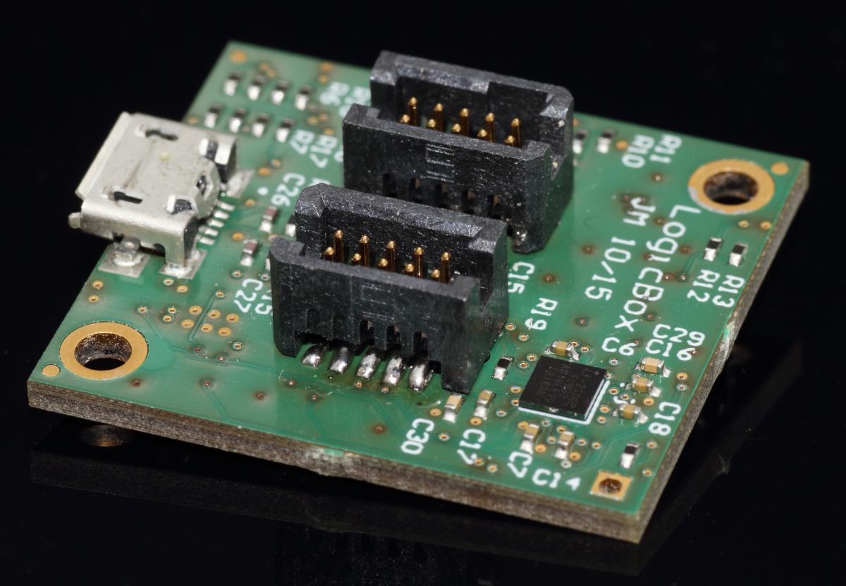
The second image is a close-up of the main board - the smallest FPGA module in the TRB family. It was already successfully used as 9-channel TDC with 500 ps binning - albeit limited in rates due to the slow connection to the PC via UART and USB.