Tip of the week: Know your limits
The buffers in all FPGAs to store data are quite large to offer some flexibility, but in most applications it makes sense to constrain the maximum amount of data:
- The ring buffers in each TDC channel can store up to 124 words - if these are filled by noise data it may generate more than 60 us of dead time for each trigger to scan the buffers for relevant data
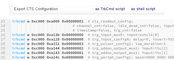
- The event buffer in each TDC can store a few thousand words in total, with a limit of typically 500 words per event ("MaxEventSize", register 0x7111)
- The size of each sub-event (data sent over one Ethernet link) is limited to 60 kB or about 15,000 TDC words. This limit can be reached or exceeded quite easily.
The TDC and TrbNet offer two levels of data limiting:
- The buffer in each TDC channel can be reduced ("DataLimit", TDC GUI, register 0xc804).
- The amount of event data generated by an individual endpoint can be limited ("SetMaxEventSize",TrbNet -> Readout, register 0x7111). This should be adjusted such that data from all channels can be transported even if TDC buffers are full and at the same time, the maximum sub-event size can not be exceeded by all endpoints connected to the same Ethernet Link.
In setups with many front-ends and low hit occupancy it can be handy to discard data from all front-ends that didn't measure any hit - The overhead from TDC headers and reference time measurement sums up to quite large amounts. The endpoints can be configured to discard all events with less than a certain amount of data ("MinEventSize", TrbNet -> Readout, register 0x7114). Setting to 5 discards all data that just contains the reference time but no other hits.
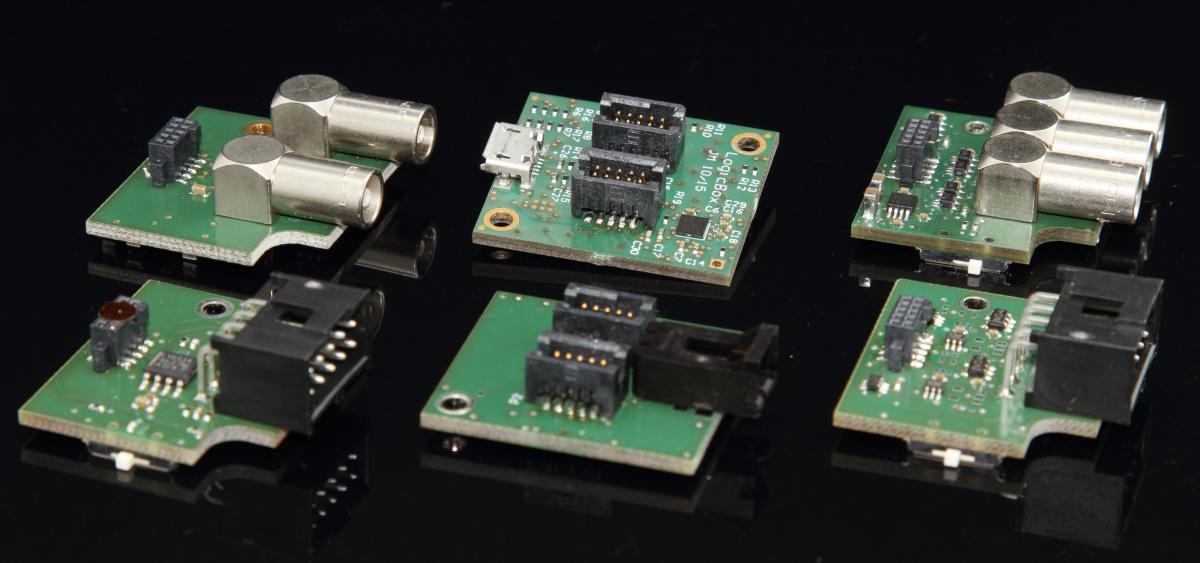
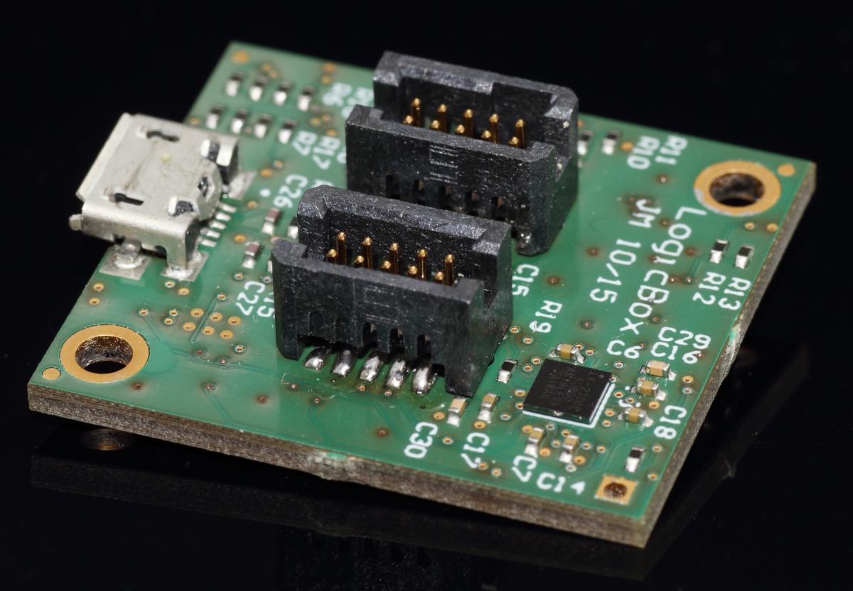
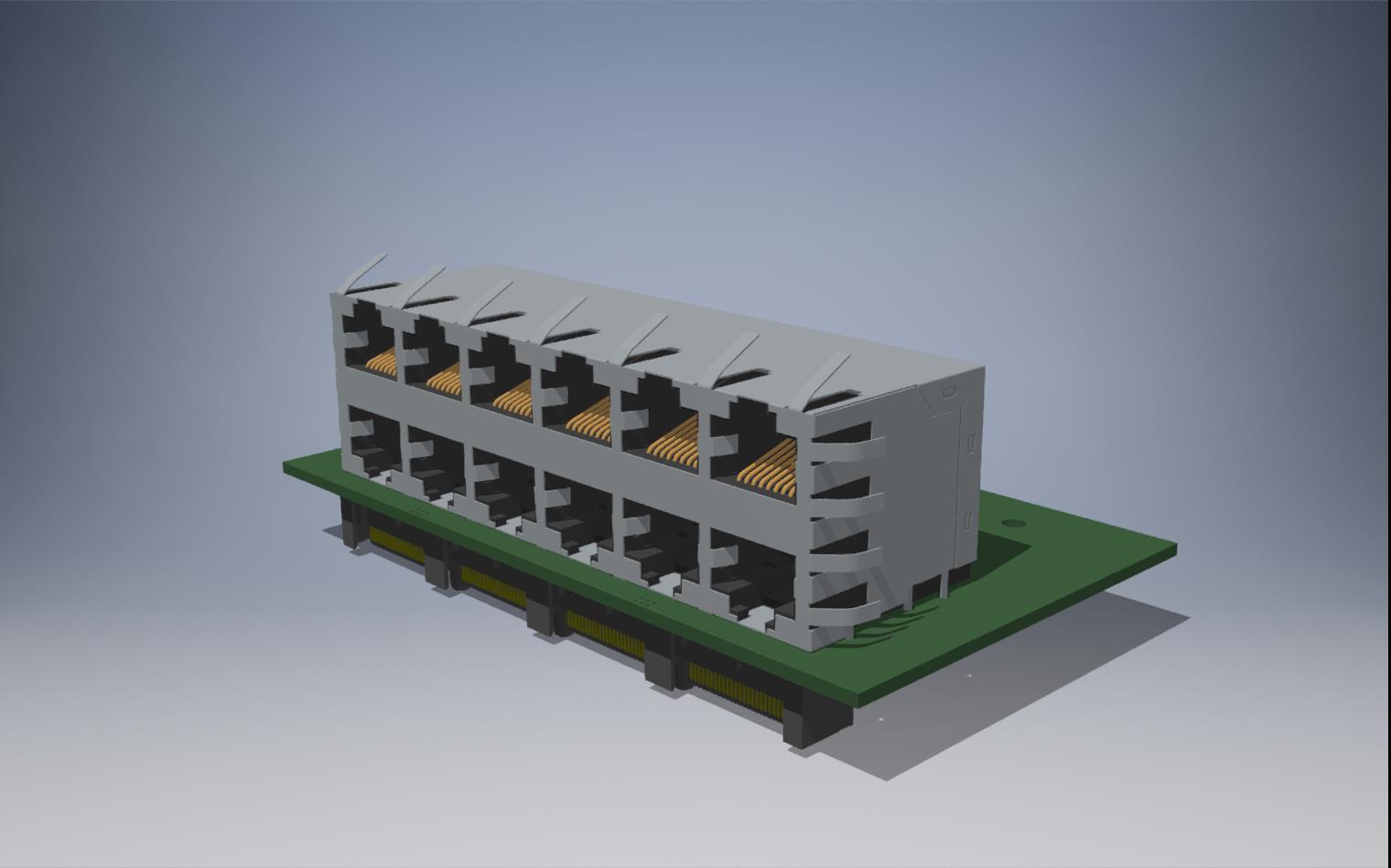 This RJ45 AddOn board provides 12 standard network cable sockets allowing to transmit the LVDS signals via shielded cables (CAT 6, S/FTP). This reduces crosstalk and signal edge distortions on neighboring signal lines, especially for longer cables.
This AddOn board uses the PADIWA 4-conn I/O schematics. The SPI lines are either available via the RJ45 sockets or on the a separate 2x10-pin connector. Furthermore, a 3.3V and 6V connection is available via a 2x2-pin connector.
This RJ45 AddOn board provides 12 standard network cable sockets allowing to transmit the LVDS signals via shielded cables (CAT 6, S/FTP). This reduces crosstalk and signal edge distortions on neighboring signal lines, especially for longer cables.
This AddOn board uses the PADIWA 4-conn I/O schematics. The SPI lines are either available via the RJ45 sockets or on the a separate 2x10-pin connector. Furthermore, a 3.3V and 6V connection is available via a 2x2-pin connector.